|
|
- A Logic Circuit Simulation Library in C++ |
|
|
- A Logic Circuit Simulation Library in C++ |
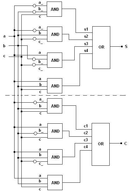
Let a and b be input signals to a 1-bit fulladder, and c the carry input. Let S be the sum output, and C the carry output. Then, the truth table for S and C, and the corresponding logic diagram, are shown below.
a  |  b  |  c  |      S  |  C
---|-----|-----|---------|----
0  |  0  |  0  |      0  |  0
---|-----|-----|---------|----
0  |  0  |  1  |      1  |  0
---|-----|-----|---------|----
0  |  1  |  0  |      1  |  0
---|-----|-----|---------|----
0  |  1  |  1  |      0  |  1
---|-----|-----|---------|----
1  |  0  |  0  |      1  |  0
---|-----|-----|---------|----
1  |  0  |  1  |      0  |  1
---|-----|-----|---------|----
1  |  1  |  0  |      0  |  1
---|-----|-----|---------|----
1  |  1  |  1  |      1  |  1

#include <lcs/or.h>
#include <lcs/and.h>
#include <lcs/not.h>
#include <lcs/tester.h>
#include <lcs/simul.h>
#include <lcs/changeMonitor.h>

// All classes of the libLCS are defined in the namespace lcs.
using namespace lcs;

int main(void)
{
    // Each node in the circuit corresponds to a single line Bus object
    // in the case of libLCS. Hence we declare a single line bus for each
    // of the nodes marked in the above circuit diagram.
    Bus<1> a, b, c, a_, b_, c_, S, C, s1, s2, s3, s4, c1, c2, c3, c4;

    // Initialising NOT gates which obtain the inverses of the input busses.
    Not<> n1(a_, a), n2(b_, b), n3(c_, c);

    // Initialising an AND gate for each of the 8 min-terms involved. Each
    // AND should take 3 input data lines. Hence, the class And<3> is used.
    // Moreover, the input busses to these AND gates should have 3 lines each.
    // Hence, the 3 line input busses are generated using the overloaded
    // '*' operator. The '*' does not denote a multiplication (or a logical AND),
    // but is a bus/line concatenation operator. It concatenates two busses
    // to produce another bus which contains lines from both the operand busses.
    And<3> sa1(s1, a_*b_*c), sa2(s2, a_*b*c_), sa3(s3, a*b_*c_), sa4(s4, a*b*c);
    And<3> ca1(c1, a_*b*c), ca2(c2, a*b_*c), ca3(c3, a*b*c_), ca4(c4, a*b*c);

    // Initialising the 4-input OR gates which take the outputs of the AND gates
    // and produce the desired results.
    Or<4> so(S, s1*s2*s3*s4), co(C, c1*c2*c3*c4);

    // Initialising a tester object which feeds a different value on to the input
    // busses at every clock pulse. This a way to feed inputs to our circuit for
    // the purpose of testing it.
    Tester<3> tester(c*b*a);

    // Initialising change monitors which monitor the changes to the busses of
    // interest. Here, we initialise monitors which report the changes on the
    // input and output busses.
    ChangeMonitor<3> inputMonitor(c*b*a, "Input");
    ChangeMonitor<2> outputMonitor(S*C, "Sum");

    Simulation::setStopTime(1000); // Set the time upto which the simulation should run.
    Simulation::start();           // Start the simulation.
    Simulation::terminate();       // Terminate the simulation space gracefully.

    return 0;
}
The output when the above program is compiled and run is as below. See this for information on interpreting the output.
At time: 0,     Input: 000
At time: 0,     Sum: 00
At time: 200,   Input: 001
At time: 200,   Sum: 01
At time: 300,   Input: 010
At time: 400,   Input: 011
At time: 400,   Sum: 10
At time: 500,   Input: 100
At time: 500,   Sum: 01
At time: 600,   Input: 101
At time: 600,   Sum: 10
At time: 700,   Input: 110
At time: 800,   Input: 111
At time: 800,   Sum: 11
