|
- A Logic Circuit Simulation Library in C++ |

|
- A Logic Circuit Simulation Library in C++ |
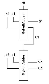
The aim of this example is it to be able to build a 2-bit fulladder using two 1-bit fulladder modules as shown below.

The 1-bit fulladder module should be built using the off-the-shelf logic gates in libLCS. The code is as follows.
#include <iostream>
#include <lcs/or.h>
#include <lcs/and.h>
#include <lcs/not.h>
#include <lcs/tester.h>
#include <lcs/simul.h>
#include <lcs/changeMonitor.h>

// All classes of the libLCS are defined in the namespace lcs.
using namespace lcs;

using namespace std;

// Define a class MyFullAdder. Our 1-bit fulladder modules will be instances
// of this class.
class MyFullAdder
{
public:
    // The constructor should take single line Bus<1> objects as inputs, one each for
    // the two data lines, carry input, sum output and the carry output.
    MyFullAdder(const Bus<1> &S, const Bus<1> &Cout,
              const Bus<1> &A, Bus<1> &B, Bus<1> &Cin);

    // The destructor.
    ~MyFullAdder();

private:
    // a, b, c are the two data inputs and the carry input respectively.
    Bus<1> a, b, c;

    // s is the sum output, and cout is the carry output.
    Bus<1> s, cout;

    // A pointer member for each of the gates which constitute our FullAdder.
    // The number and type of the gates is same as in the 1st basic example.
    Not<> *n1, *n2, *n3;
    And<3> *sa1, *sa2, *sa3, *sa4;
    And<3> *ca1, *ca2, *ca3, *ca4;
    Or<4> *so, *co;
};


MyFullAdder::MyFullAdder(const Bus<1> &S, const Bus<1> &Cout,
                     const Bus<1> &A, Bus<1> &B, Bus<1> &Cin)
         : a(A), b(B), c(Cin), s(S), cout(Cout)
{
    Bus<> a_, b_, c_, s1, s2, s3, s4, c1, c2, c3, c4;

    // Each of the gates should be initialised with proper bus
    // connections. The connections are same as in the 1st basic
    // example.

     // Initialising the NOT gates.
    n1 = new Not<>(a_, a); n2 = new Not<>(b_, b); n3 = new Not<>(c_, c);

    // Initialising the AND gates for the
    // minterms corresponding to the sum output.
    sa1 = new And<3>(s1, (a_,b_,c)); sa3 = new And<3>(s3, (a,b_,c_));
    sa2 = new And<3>(s2, (a_,b,c_)); sa4 = new And<3>(s4, (a,b,c));

    // Initialising the AND gates for the
    // minterms corresponding to the carry output.
    ca1 = new And<3>(c1, (a_,b,c)); ca2 = new And<3>(c2, (a,b_,c));
    ca3 = new And<3>(c3, (a,b,c_)); ca4 = new And<3>(c4, (a,b,c));

    // Initialising the OR gates which
    // generate the final outputs.
    so = new Or<4>(s, (s1,s2,s3,s4)), co = new Or<4>(cout, (c1,c2,c3,c4));
}

MyFullAdder::~MyFullAdder()
{
    // The destructor should delete each of the gates
    // which were initialised during construction.

    delete n1; delete n2; delete n3;
    delete sa1; delete sa2; delete sa3; delete sa4;
    delete ca1; delete ca2; delete ca3; delete ca4;
    delete so; delete co;
}

int main(void)
{
    // Declaring the busses involved in out circuit.
    // Note that the bus c0 (the carry input to the first full-adder)
    // has been initialised with a value of 0 (or lcs::LOW) on its line.
    Bus<> a1, b1, a2, b2, c0(0), S1, C1, S2, C2;

    // Initialising the 1-bit full adder modules.
    MyFullAdder fa1(S1, C1, a1, a2, c0), fa2(S2, C2, b1, b2, C1);

    // Initialising monitor objects which monitor the inputs and the
    // 3 sum bits.
    ChangeMonitor<4> inputMonitor((a1,b1,a2,b2), "Input", DUMP_ON);
    ChangeMonitor<3> outputMonitor((S1,S2,C2), "Sum", DUMP_ON);

    // Initialising a tester object which feeds in different inputs
    // into our circuit.
    Tester<4> tester((a1,b1,a2,b2));

    Simulation::setStopTime(2000); // Set the time upto which the simulation should run.
    Simulation::start();           // Start the simulation.

    return 0;
}
When the above code is compiled and run, the following output is obtained.
At time: 0,     Input: 0000
At time: 0,     Sum: 000
At time: 200,   Input: 0001
At time: 200,   Sum: 001
At time: 300,   Input: 0010
At time: 300,   Sum: 010
At time: 400,   Input: 0011
At time: 400,   Sum: 011
At time: 500,   Input: 0100
At time: 500,   Sum: 001
At time: 600,   Input: 0101
At time: 600,   Sum: 010
At time: 700,   Input: 0110
At time: 700,   Sum: 011
At time: 800,   Input: 0111
At time: 800,   Sum: 100
At time: 900,   Input: 1000
At time: 900,   Sum: 010
At time: 1000,  Input: 1001
At time: 1000,  Sum: 011
At time: 1100,  Input: 1010
At time: 1100,  Sum: 100
At time: 1200,  Input: 1011
At time: 1200,  Sum: 101
At time: 1300,  Input: 1100
At time: 1300,  Sum: 011
At time: 1400,  Input: 1101
At time: 1400,  Sum: 100
At time: 1500,  Input: 1110
At time: 1500,  Sum: 101
At time: 1600,  Input: 1111
At time: 1600,  Sum: 110
Below is the screenshot of the gtkwave plot of the generated VCD file.

